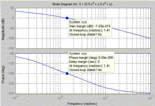
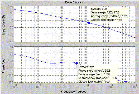
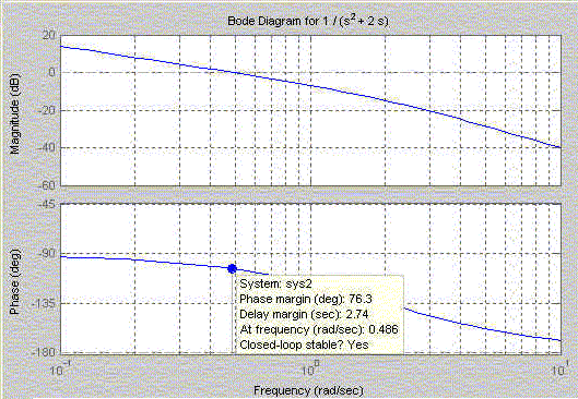
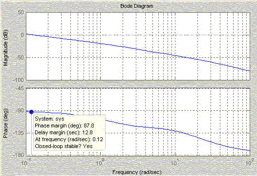
BODE:
LAG COMPENSATION:
Transfer function of Lag compensator:
s + 0.1
----------
10 s + 0.1
LEAD COMPENSATION:
Transfer function of compensator:
s + 4.41
--------
s + 18.4
LEAD - LAG COMPENSATION:
Lead Type Circuit: FLead(s) = K*N (s + b) / (s + bN)
Lag Type Circuit: FLag(s) = (s + a) / (s + a/M)
Design Procedure for a Lead-Lag Compensator:
- First we design the Lead part of the compensator then the Lag part of the compensator.
- Plot open loop transfer function of uncompensated plant and decided how much gain and phase are required at the particular frequency of interest.
- Add 6 deg to the extra phase lag to the value obtained from the open loop uncompensated system frequency response.
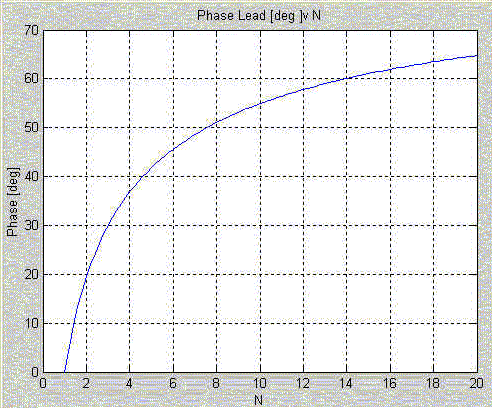
- From Figure1 below decided what value of N to select based on the total amount of phase required.
- To obtain b so as to give the maximum phase
at the desired frequency wd
use the formula
wd = b * √(N)
- To calculate K use the formula K*√(N)*G(wd*wd)
- To calculate the lag filter parameter a use a = 0.1*wd
- To calculate the lag filter parameter M use final value theorem and steady state error margin